This section is a comprehensive resource for all hardware and software details related to the DIY stereo integrated amplifier that comprises Project Artemis.
DISCLAIMER
Information here is provided as-is without warranties, based on my current understanding. While efforts are made for accuracy, errors may exist and information may change over time.
Caution: Handling mains AC voltages can be dangerous, potentially causing injury or damage. If unsure about electrical work, seek professional advice. I’m not liable for any harm or damage resulting from actions taken based on this content. Always prioritize safety.
Significant time has been invested in this project; please respect this effort by not exploiting it for financial gain.
Materials are intended for personal use under no license. Commercial use is prohibited.
By engaging with Project Artemis in any way, you implicitly accept these terms, whether you’ve read them or not.
INFO
This DIY project involves a custom-built, integrated amplifier developed from scratch, currently in a functional prototype stage despite a few minor bugs. Originating in late 2015 with actual work beginning in 2016, it has undergone numerous iterations, each PCB was revised multiple times.
This amplifier isn’t suitable for beginners; it requires knowledge in programming, PCB design, Bluetooth LE, and electrical and audio engineering. While replicating it exactly may be challenging due to the use of specific components from my audio equipment, like transformers and the case from a Pioneer A-10 amplifier acquired at a low cost, the project offers valuable information about the design and engineering process.
Project has been a labor of love over several years, interspersed with significant life events, including marriage and children, all while managing a full-time job.
Currently, I lack the equipment to measure specific metrics like THD and power output, though simulations have been done in LTspice. Given the high cost of lab equipment and the project being a non-profit endeavor, detailed specifications remain unknown.
CONCEPT | FEATURES
Project is a high-end, custom-built integrated amplifier that rivals, and in many aspects surpasses, the standard offerings found on the market today. This project was born from the ambition to create a fully functional, aesthetically pleasing device that delivers superior sound quality while including all the functionalities typical of high-end audio equipment, along with some innovative additions.
Key Features:
Selectable Inputs: Relay-based input selection for audio source switching.
Custom DAC: Features a custom-developed DAC with an auto power-off function when not in use.
Mute Functionality: A relay-based mute function.
Motorized Volume and Tone Control: Equipped with a 4-channel ALPS potentiometer for volume and 6-channel ALPS pots for tone control, both with ADC readings for precise control.
Tone Bypass: Relay-based tone bypass for clear audio playback.
Enhanced Bass Boost: Discrete bass boost circuit inspired by Onkyo schematics for deep, rich bass.
Premium Pre-amplifier and Power Amplifier: Features discrete Current Feedback Amplifier (CFA) designs for both pre-amplifier and power amplifier stages, drawing inspiration from Marantz schematics, extensive online research and LTspice simulation tweaking.
Bluetooth® Low Energy (BLE) Connectivity: Offers BLE connection to Android devices for remote control and monitoring, powered by an nRF52 module.
Infrared (IR) Remote Control: Supports IR remote control for remote operation.
Exclusive Android Application: Comes with a custom-developed Android app tailored for this project.
Standby and Power Features: Includes standby circuitry and dual power transformers for dual current capacity.
Dedicated Power Circuitry: Separate power supplies for the pre-amp, DAC, relays, and digital components ensure best sound quality.
Protection Circuitry: Equipped with DC output and power supply voltage asymmetry protection.
Temperature Monitoring and Protection: Features TMP100 IC for temperature monitoring and safeguards against overheating.
LED Features: Offers LED dimming and a distinctive LED on the volume knob for a modern, sleek look.
Current Limitations and Future Possibilities:
Headphone Output: Although a connector is integrated, it remains unconnected as it wasn’t deemed necessary for the initial design.
Coaxial Inputs for DAC: Omitted based on the current needs.
Bluetooth Audio Streaming: Not included due to additional module and coding requirements.
USB Input: Excluded from the design.
Phono Input: Not part of the current configuration.
These features might be considered for future updates, but given the long development and implementation process, their inclusion remains uncertain.
PROJECT DETAILS
The project is divided into two main categories: hardware and software, catering to a broad audience of technology enthusiasts and professionals. The hardware aspect is presented by its PCB components, showcasing the project’s hardware engineering. On the software front, it contains projects tailored for microcontrollers (MCUs) like STM32 and nRF52, as well as Android application, appealing to developers in embedded systems and mobile app development.
HARDWARE
STANDBY PCB
The simplest PCB within the project, incorporates a standby power transformer and voltage regulators needed for the MCU and digital components across other boards. Sourced from a Pioneer A-10 integrated amplifier, the low-power standby transformer (~2VA) primarily follows the original device’s schematics, delivering milliamp-range currents.
The board is designed to supply voltage immediately upon connection to an AC outlet, providing both +3.3V and +5V outputs to support the project’s ICs. It features a relay for activating power transformers, rated at 250VAC 16A, ensuring safe handling of mains AC voltages. Design allows the standby transformer to be bypassed when the main power transformers are activated.
Key components powered by the standby +3.3V include the STM32 MCU, Bluetooth nRF52 module, IR circuitry, and a standby LED. The choice of a modestly powered transformer minimizes standby power consumption, aligning with EU regulations for energy efficiency, an essential consideration for those aiming to professionalize their projects.
TopBottom
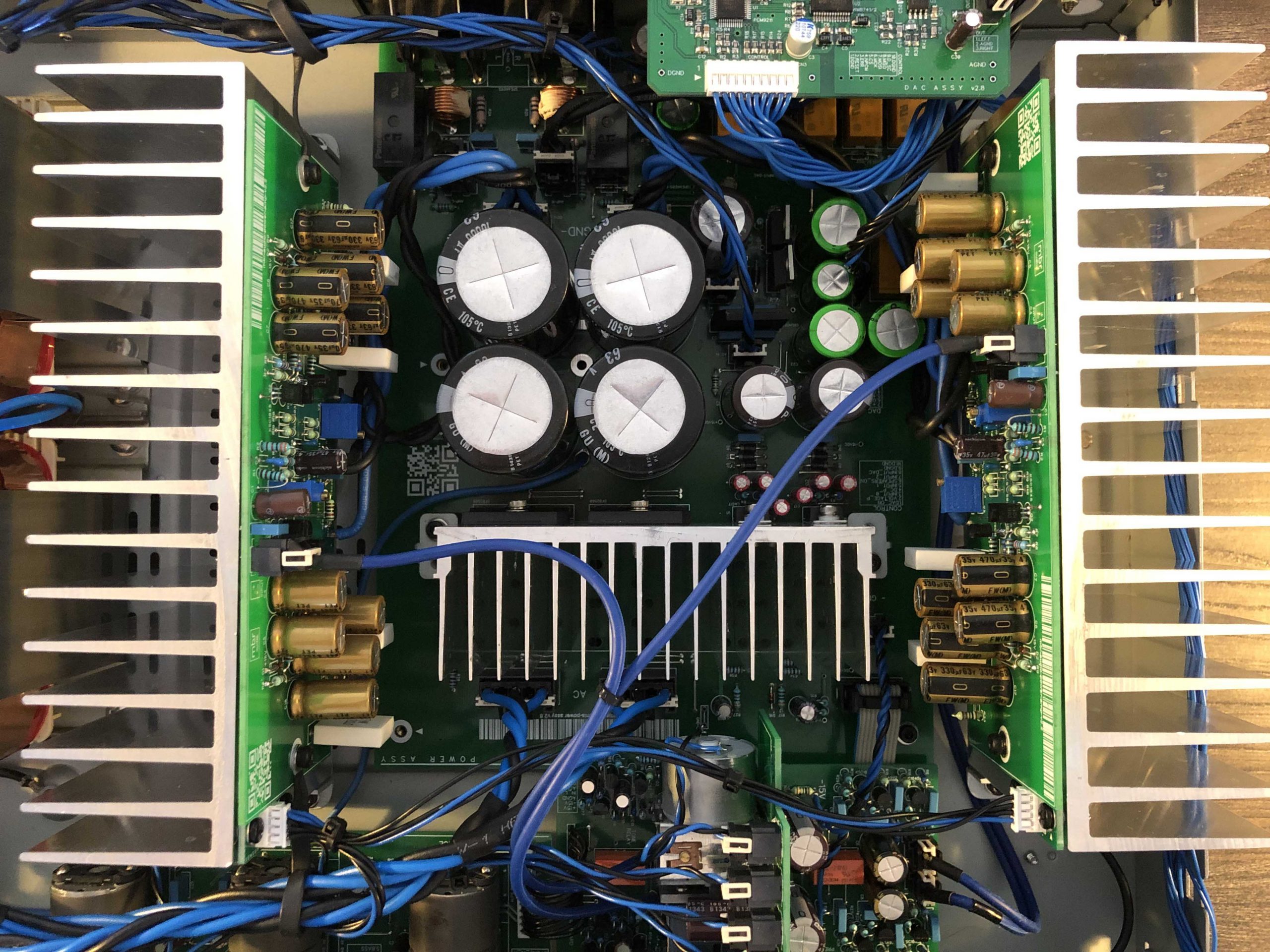
POWER PCB
This board is a comprehensive hub for the amplifier, integrating power supplies, protection circuits, and connectors for both input and speakers. It features a dual-rectifier power supply for the amplifier, equipped with two 16A rectifiers and enhanced by two pairs of 10000uF/63V capacitors. This setup ensures a stable ±40V DC output, supported by two parallel-connected power transformers to double current capacity, each estimated at 150VA.
The pre-amplifier’s power is regulated by an LM317/LM337 combination, with additional filtration and voltage adjustment components ensuring a reliable ±15V output. The relay and DAC power supplies include their specific regulators and capacitors. DAC power supply incorporates an on/off switching mechanism inspired by Marantz PM6005/6006 models.
Protection features on the board include voltage balance and DC protection circuits, signaling any anomalies to the MCU to immediately turn off the power.
A dedicated star ground point minimizes noise across the system and is essential in audio based devices.
TopBottom
POWER AMPLIFIER PCB
This board is dedicated to the power amplifier circuit, it’s a unified PCB design for each channel to maintain consistency. Embracing the KISS (Keep It Simple Smart) principle, the aim was to develop a straightforward yet high-performing circuit that ensures long-term reliability and ease of repair.
The journey began with exploring class A designs but ultimately pivoted to class AB, drawing inspiration from renowned sources like Hiraga, Hifisonix, and Pavel Macura’s CFA amp. The final design borrows from Hifisonix’s KX-2 amp, albeit in class AB configuration, incorporating capacitance multipliers and additional adjustments based on LTspice simulations to enhance performance.
The PCB is crafted to accommodate heatsinks and fit within the specified case, highlighting a modular approach that allows for easy swapping of amplifiers. Utilizing Toshiba’s 2SC5200/2SA1943 output transistors and a combination of KSC2690/KSA1220 and KSA992/KSA1381 pairs for the driver and VAS stages, respectively, the circuit achieves a simulated output of 120W on 8 ohms and a THD of 0.002768% under ideal simulation conditions. Real-world THD might be higher due to the limitations of simulation models.
I extend my gratitude to Hifisonix, Pavel Macura, ESP (Elliot Sound Products), Bora Omega (Borina Amaterska Svaštara), Apex Audio, dadod from the DIYaudio forums, and many others for their contributions of schematics and ideas. Their extensive resources have been instrumental in enabling my ventures into audio engineering, a field where I initially felt least confident. Their dedication to sharing knowledge has been crucial for hobbyists like myself and the broader DIY audio community.
TopBottom
PRE-POWER AMPLIFIER PCB
This board features a discrete CFA pre-amplifier based on the Marantz PM6005/6006 and a discrete bass boost circuit derived from the Onkyo A-9150. Designed to complement a CFA power amplifier, the pre-amp is similar to its Marantz origins, with minor component adjustments. The bass boost provides a significant lift of approximately 9dB at 30Hz, enriching the low-end frequencies for a better sound profile.
Incorporating three relays, the board allows users to toggle bass boost, mute, and direct (tone bypass) modes, ensuring a direct signal path from input to output. The PCB underwent several revisions for optimal layout, integrating 1000uF/35V capacitors with 10-ohm resistors for stable power delivery to both the pre-amp and bass boost circuits.
The volume control PCB attaches vertically, creating a compact assembly.
TopBottom
VOLUME PCB
This board is centered around a 4-channel 50k ALPS RK27 potentiometer, utilizing two channels for precise volume control and the remaining two to interface with an ADC for potentiometer position calculation. Given the logarithmic nature of the pot, ADC tracking presents challenges, so a coded solution is in place and went several changes for accuracy improvement.
The board features Toshiba TB6552D dual bridge drivers and a Microchip MCP23008 port expander to manage these drivers via I2C communication from the main MCU. This setup supports the implementation of volume and tone controls (including bass, treble, and balance) using ALPS RK16 6-channel motorized potentiometers.
Board includes a connector for integration with the pre-amplifier PCB, facilitated by a right-angle 2.54mm connector.
TopBottom
TONE PCB
This board integrates three 6-channel 50k ALPS RK16 linear potentiometers alongside tone circuitry. The design leverages 6-channel potentiometers due to the shared ground between channel pairs, facilitating left and right audio channels plus ADC tracking. Despite the challenge of sourcing these specific potentiometers, mainly available through Chinese suppliers, the components used performed well, with no issues.
Given the rarity and cost of 6-channel potentiometers, there was consideration for switching to a digital approach using the NJW1194 chip combined with three 2-channel potentiometers for future projects. This chip also offers digital volume control, suggesting a potential simplification of the volume control setup.
The board employs a classic Baxandall tone control scheme, with valuable insights gained from ESP and Bora Omega’s resources. A noted issue with the balance control, where one channel is amplified while the other is attenuated, deviating from expected behavior—remains to be addressed. However, this has not significantly impacted the project’s progress and is marked for future revision.
TopBottom
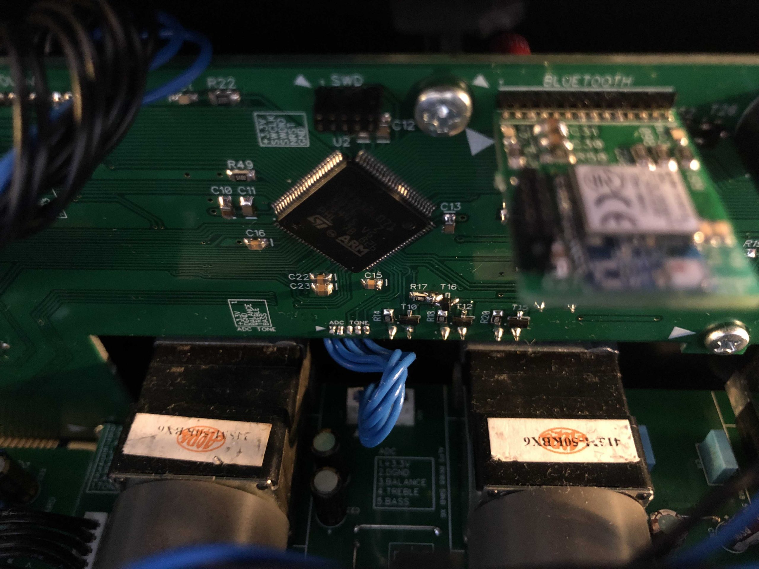
CONTROL PCB
This board is the heart of the project, powered by an STM32L071 MCU, operating all functions. It includes two auxiliary PCBs: one for a Bluetooth module and another for the TMP100 temperature monitoring IC.
TopBottom
DAC PCB
This board showcases a PCM9211 digital audio interface transceiver and a high-performance WM8742 stereo DAC, marking my foray into custom DAC design. The choice of PCM9211 was driven by its widespread use as a digital switch and optical receiver in other audio devices offered in the current market.
Board was seamlessly integrated with the STM32 MCU, benefiting from prior iterations of the Control PCB that laid the groundwork for adding DAC capabilities without complications.
SPI protocol is used for communication with both chips on the board.
TopBottom
SOFTWARE
AmpX – Android application
You can explore and download the Kotlin-based Android app for amplifier control here. Application is compatible with Android 4.3 and above and was designed initially for Android 12.
As an ongoing project, the app is stable and open for use, with all components, including custom views, designed by me. If you opt to use it, a nod of acknowledgment would be appreciated. The app’s design and icons, derived from Google’s Material Design, feature a blue theme to match the amplifier’s LED aesthetics.
Featuring a single-activity interface with a Motion Layout main view, the app allows users to toggle between volume/input and tone controls. Interactivity is a core feature, with circular dials and buttons responsive to both app and amplifier changes. It includes “Connect” and “Settings” dialogs for device scanning and personal adjustments, respectively.
The source code is available for those interested in deeper insights. While an iOS version is feasible, the lack of a Mac currently makes it impractical without funding to cover development costs.
AmpX – Android application
You can explore and ownload the C-based nRF52832 application source code here, developed with nRF5_SDK_17.1.0_ddde560. The nRF52832, a versatile Bluetooth 5.x SoC featuring a 64 MHz Cortex-M4 microcontroller, supports BLE, Bluetooth mesh, and NFC. This application, a straightforward wire replacement solution, facilitates communication between a mobile app and an STM32 MCU via the Laird BL652-SA BLE module, leveraging UART for message transmission.
This app acts as a bridge: commands from the mobile app are sent to the nRF52832, then relayed to the STM32 MCU for execution, and vice versa. Designed around the cost-effective, easy-to-solder Laird module, this setup was chosen over higher-pin alternatives to maintain simplicity and modularity, allowing for easy updates or replacements of the BLE module without altering the Control PCB.
The nRF52 platform is chosen for its future-proof nature, thanks to Nordic Semiconductor’s continuous updates and feature additions. This app serves as a versatile foundation for similar projects, available for use and adaptation, free of charge—credit appreciated.
For those venturing into BLE development, opting for a pre-certified module can significantly simplify the certification process required by regulatory bodies like the FCC, CE(RED), or NCC, avoiding the high costs associated with certifying a chip-based design.
STM32 embedded application – v4
You can explore and download the C-based application for amplifier control here, developed for the STM32L071 MCU with 100 pins using STM32CubeIDE v1.7.0. The source code is available for free use, with a request for credit if utilized. Despite some pending issues and improvements, including a misfiring protection feature and updates for the mobile app, the application is stable and functional.
Key features include:
Input switching via relays with a delay mechanism to prevent rapid on/off cycles when using the rotary encoder.
An IR receiver driver, functional but requires optimization.
A comprehensive power-on sequence.
LED brightness control through PWM.
Drivers for the rotary encoder, SPI PCM9211, SPI WM8742, Bluetooth UART, and TMP100 I2C with dual ICs on a single bus.
Button interfacing through a resistor ladder to ADC.
ADC integration for motorized potentiometer readings.
An I2C driver for the MCP23008 port expander.
Protection circuit management, working but needs further testing and refinement.
Titled as the fourth version, this iteration aligns with the fourth revision of the Control PCB, representing an iterative development.
Images taken from the web are in the ownership of their respective companies.
Bluetooth Low Energy PCB with nRF52 module. Below is tone control PCB with motorized potentiometers.Overview of the entire project.Power supplies for amplifiers, pre-amp and DAC.Power amplifier.Heart of everything, STM32L071 MCU.Standby power PCB and power transformers.Volume control PCB. Lower PCB is discrete pre-amp and bass boos circuit.Custom DAC based on PCM9211 and WM8742.Bass boost ciruit below, vertical PCB has motor control circuitry.